
High Voltage MOSFET Driver
Driving a high-side MOSFET is more of a challenge than you might think, because of several characteristics and limitations that they have. In addition, off the shelf MOSFET driver chips are often limited by their supply voltage to under 20V.
One limitation is the gate to source voltage Vgs which typically can not exceed 20V. This becomes a particular problem when driving high-side MOSFETs because they can't be driven with a voltage that spans a high voltage supply, e.g. supplies greater than 20V.
Another characteristic that makes driving MOSFETs difficult is input gate capacitance Ciss is normally proportional to its rated current. Large power MOSFETs have large input capacitance. Thus, the circuit which drives a MOSFET must overcome this input capacitance.
Another issue that must be resolved by the driver is minimization of simultaneous conduction of complementary pairs of MOSFETs as they transition states. A "dead-time" where one transistor is delayed in turning on until the other turns on is needed to prevent current flow through both transistors, which create spikes and makes them overheat.
The circuit below is a high voltage MOSFET driver. The author has built and tested this circuit, and it will pass a pulse trains faster than 1MHz. It will handle voltages greater than Vgs. For voltages greater than 40V the resistor values need to be changed such that Vgs(max) is never exceeded. This is a simple task since they are all just voltage dividers. One disadvantage of the circuit is that it has a high quiescent current. Even when the circuit is not being driven with pulses, the resistors still have current flowing through them.
The transistors should be chosen to minimize the input capacitance.
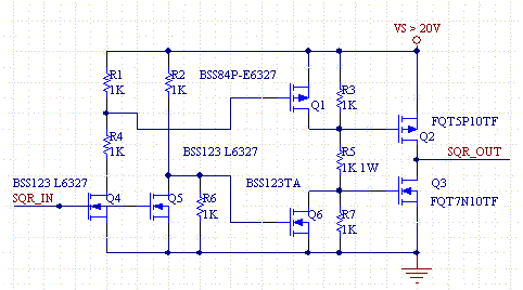
Figure 1. High Voltage MOSFET Driver with Minimized Cross-Over Current.
The following circuit is for supply voltages that are less than Vgs. It is advantageous over the above circuit, in that fewer components are needed and it draws less power, because some of the resistors are not needed. D1 is a Zener whose voltage is Vs-Vd. When Q10 turns on both gates are grounded, and Q7 is on and Q11 is off. When Q10 turns off, a voltage forms across R8,R11 and D1. Select the resistors such that VR8<Vth so that Q7 of off, and VR 11 >Vth so that Q11 is on. This should occur when R8<R11 and the zener voltage rating is Vs-Vd.
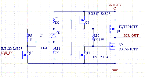
Figure 2. Low Voltage MOSFET Driver with Minimized Cross-Over Current.
What's amazing about both of these circuits is how they minimize cross-over current by elegantly incorporating dead-time. The resistor that sits between the drains of the driver MOSFETs limits the current when both transistors are conducting, which improves efficiency.
In addition, this same resistor combined with the input capacitance of the output MOSFETs, forms a time constant which prevents them from turning on at the same time. When Q11 of Figure 2 turns on, Q9 which was conducting is forced off almost immediately because Q11 has low impedance, where as Q8 take time before it turns on because it's gate capacitance must charge through R10. Likewise when Q7 turns on, Q8 is immediately turned off, and Q9 slowly turns on because of the limited current flow due to R10 and it's own input capacitance. The result is that the circuit automatically inserts dead time. R10 conducts at all times and so it must be chosen with a power rating twice the other resistors. It's power is:
P= (VS/2)^2/R;