
Inrush Current Limiting Load Switch Calculator
Inrush current occurs when power is applied to a circuit, in particular circuits with capacitive loads. As the capacitive load charges it creates a current spike, and corresponding voltage dip on the power supply input, due to the internal resistance of the battery or power supply. Normally this isn't a problem at start up, and it is assumed that there will be some settling time required when power is applied. For example, most microcontrollers are kept in a reset state until power has stabilized. However, in rush current becomes more of a problem, when power is switched to a capactive load some time after the initial power has been applied, because the in rush current and supply voltage dip if severe enough can cause microcontrollers to reset or brown out.
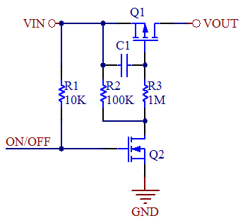
There are various ways to mitigate in rush current. The following circuit, called a "load switch" uses 2 transistors to mitigate inrush current. The circuit exploits the gate capacitance of MOSFETS. When power is off both transistors are off, because R2 pulls the gate of Q1 high, such that Vgs is 0V. When power turns on Q2 turns on, and in turn pulls the gate of Q1 low through R3, a weak resistor. R3 and the gate capacitance form a time constant circuit. The power FET Q2 turns on slowly, limiting the inrush current, and in turn reducing voltage dip of the supply. An optional capacitor C3 can be added to the gate and source of the power transistor to increase gate capacitance and allow a smaller gate resistor R3 to be used. The capacitor also reduces the variance of the time constant across different transistors that may have a variance in the gate capacitance.
The power supply voltage dip is a function of the internal resistance of the battery, or voltage supply, and the capacitance of the load:
I(in rush)= C(load)*dv/dt;
V(dip)= I(in rush)*R(internal resistance);
V(dip)= R*C*dv/dt;
For example suppose we have a discharged 10uF capacitive load, and a 9V battery with a nominal internal resistance of 2 ohms. Suppose we flip a switch to apply power to the load. In this case, dv= 9v, and suppose that dt is limited by the inductance of the wire, and is 2.5uS. I(in rush)= 10*9/2.5= 3.6A. The voltage dip in this case could be as high as 7.2V (3.6A*2ohms). If the load had a much greater capacitance say 100uf, then the limiting factor of the current would be the internal resistance of the battery or power supply.
When designing the in rush current limiting load switch, find the gate capacitance of the power FET from its data sheet, and measure the width of the power pulse with a scope. The goal is to decrease the depth of the voltage dip, by increasing it's width as a trade off. Thus, the time constant of the power FET Q2 and its base resistor should be much greater than the duration of the un-mitigated voltage dip, a factor of ten greater is a good starting point.